Project Gallery
Laser cutting uses a focused, high-energy beam to melt, vaporise, or ablate material along a programmed path, producing clean, burr-free edges with very tight dimensional control and no tool wear.
From UV cold-cutting of brittle ceramics and PCB materials to high-power fiber laser cutting of copper and stainless steel, Monotek Photonics supplies the right laser source and integration support for precision and production-scale cutting applications.
Compatible Materials
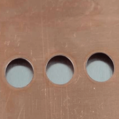
CW or quasi-CW laser melts the material while assist gas removes the molten zone to create a clean kerf on metals.
UV nanosecond or picosecond laser vaporises material layer-by-layer with minimal thermal load on brittle substrates.
Focused internal modification allows wafers or glass to separate with minimal kerf loss and very low surface damage.
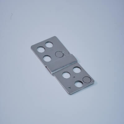
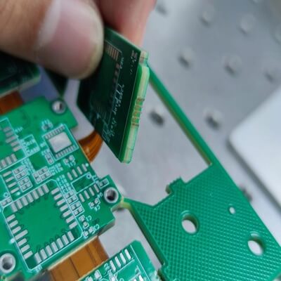
Z-depth control enables cutting of specific layers in multilayer boards or composite structures without damaging adjacent layers.
Galvo and stage-based systems deliver micron-level positional accuracy far beyond punching, routing, or waterjet alternatives.
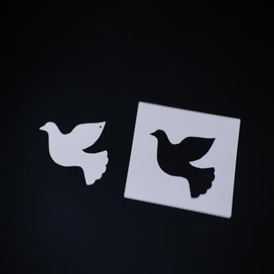
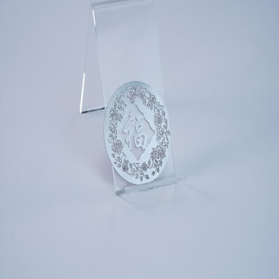
High PrecisionComplex profiles, inner cutouts, sharp corners, and micro-features are software-defined with no tooling change required.
Flexible DesignUV and picosecond sources cut ceramics, polymers, and films with extremely low heat-affected zone and excellent edge quality.
Clean FinishPrecise depth control allows selective layer removal in boards and composites without disturbing neighboring structures.
Process ControlPrecision cutting of PCB, FPC, wafers, and electronic films for miniaturized and high-density assemblies.
Cold cutting of brittle materials such as ceramics, sapphire, and glass with minimal cracking and high edge quality.
Cutting of copper, stainless steel, aluminium, and precision foils for industrial and fabrication workflows.
Selective and low-damage cutting of layered structures, advanced films, CFRP, and engineered substrates.
Copyright © Monotek Photonics India Pvt. Ltd., All Rights Reserved.
Designed By Monotek Photonics